Q&A: A high-tech take on Wagner’s “Parsifal” opera
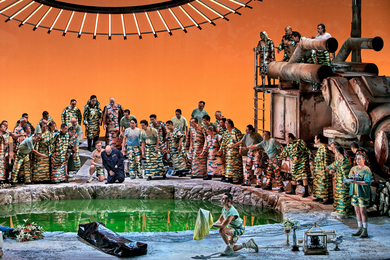
Director and MIT Professor Jay Scheib’s production, at the Bayreuth Festival in Germany, features an apocalyptic theme and augmented reality headsets for the audience.
Director and MIT Professor Jay Scheib’s production, at the Bayreuth Festival in Germany, features an apocalyptic theme and augmented reality headsets for the audience.
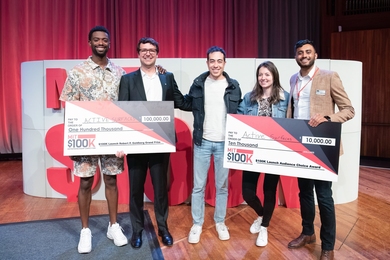
The founders of MIT spinout Active Surfaces describe their thin-film solar technology and their experience winning this year’s $100K.
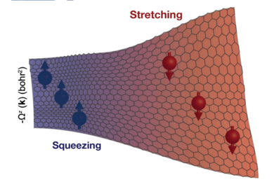
Researchers discover how to control the anomalous Hall effect and Berry curvature to create flexible quantum magnets for use in computers, robotics, and sensors.
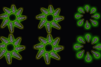
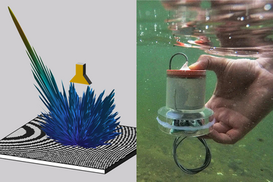
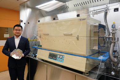
A new technique produces perovskite nanocrystals right where they’re needed, so the exceedingly delicate materials can be integrated into nanoscale devices.
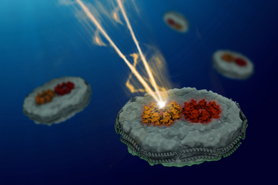
The disorganized arrangement of the proteins in light-harvesting complexes is the key to their extreme efficiency.
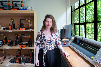
MIT Morningside Academy for Design Fellow Ganit Goldstein SM ’23 combines traditional craftsmanship and technology to transform the way clothes are produced and worn.
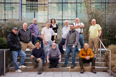
All together, a core group of MIT.nano staffers has more than 400 years of technical experience in nanoscale characterization and fabrication.
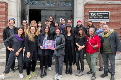
Over the course of four days, Indigenous delegates collaborated on immersive technology with MIT community members.
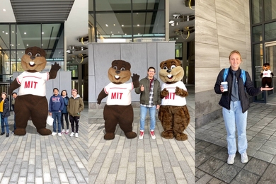
MIT student creates Tim the Beaver in virtual reality using the MIT.nano Immersion Lab.

The Fulbright US Student Program funds opportunities for research, graduate study, and teaching abroad.
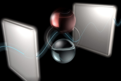
A perovskite-based device that combines aspects of electronics and photonics may open doors to new kinds of computer chips or quantum qubits.
The HUMANS nanowafer, an MIT Space Exploration Initiative student-led project, will travel to the ISS this month, and later to the moon, carrying messages in more than 64 languages from over 80 countries.

A campus summit with the leader and his delegation centered around dialogue on biotechnology and innovation ecosystems.
A new low-temperature growth and fabrication technology allows the integration of 2D materials directly onto a silicon circuit, which could lead to denser and more powerful chips.